Why Every Semiconductor Device You’ve Ever Used Depends on One Quiet Boundary
In a chunk of silicon no bigger than a grain of sand, something remarkable happens at the exact line where two differently doped crystals meet. No moving parts. No sound. Just a region — invisible to the naked eye — that decides whether current flows or doesn’t. That boundary is the PN junction, and without it, there would be no transistors, no diodes, no LEDs, no solar cells, no modern electronics.
If you’ve ever wondered why your phone’s processor works, or why a solar panel generates electricity when light hits it, or why an LED glows a specific color — the answer is always the same: the PN junction.
The Problem: Silicon Wants to Be Neutral
A pure silicon crystal has a perfectly balanced lattice — every silicon atom shares its four valence electrons with its four neighbors, forming strong covalent bonds. There are no free electrons wandering around, which makes pure silicon an excellent insulator at room temperature.
But doping changes everything. Doping is the controlled process of adding trace amounts of other elements into the silicon lattice:
– N-type silicon is doped with phosphorus or arsenic, which have five valence electrons. Four of them form bonds with neighboring silicon atoms, leaving one electron nearly free to roam. The material now has excess negative charge carriers.
– P-type silicon is doped with boron or gallium, which have only three valence electrons. This creates “holes” — vacant positions where an electron could be, but isn’t. These holes act as positive charge carriers.
Both materials start neutral overall. But at their boundary, things get interesting.
The Junction: Where Two Worlds Collide
When you place P-type and N-type material next to each other, the electrons from the N-side immediately see the holes on the P-side and start diffusing across the boundary to fill them. This is called diffusion current.

Every electron that crosses leaves behind a positively charged ion on the N-side. Every hole that gets filled leaves behind a negatively charged ion on the P-side. These fixed ions can’t move — they’re locked in the crystal lattice. Over a region spanning roughly a micrometer or two, a depletion region forms, populated only by these immobilized charges.
This build-up of fixed charges creates an electric field and a corresponding built-in potential (V_bi). At equilibrium, the built-in potential exactly opposes further diffusion. The depletion region stops growing when the electric field is strong enough to sweep charge carriers back across the junction as fast as diffusion pushes them in.
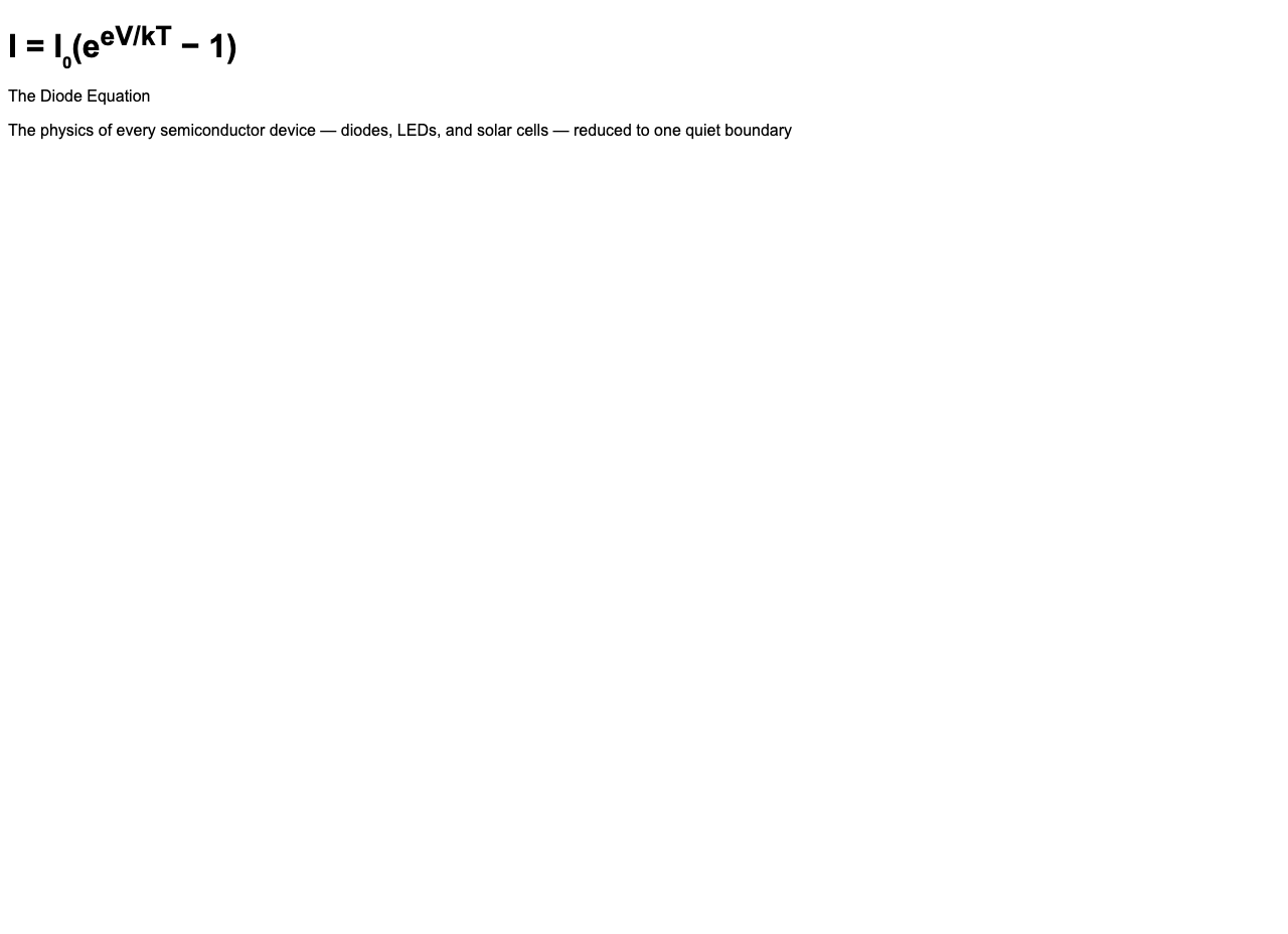
The key equation is the diode equation, which describes the current-voltage behavior:
I = I₀(eeV/kT − 1)
Where I₀ is the tiny reverse-bias saturation current (typically ~10⁻¹⁴ A for silicon), e is the electron charge, V is the applied voltage, k is Boltzmann’s constant, and T is temperature. At room temperature (300 K), kT/e ≈ 26 mV — the characteristic thermal voltage.
Forward Bias: When the Barrier Falls
When you connect the P-side to the positive terminal of a battery and the N-side to the negative terminal, you apply a forward bias. The external voltage reduces the built-in potential. As V increases toward the diode’s turn-on voltage (~0.6–0.7 V for silicon), the depletion region narrows. Once the barrier is sufficiently reduced, electrons from the N-side can cross into the P-side (and holes from P into N) easily, and current flows exponentially.

The exponential in the diode equation means that for every 60 mV increase in forward voltage at room temperature, the current roughly tenfold increases. The relationship is dramatic: a diode at 0.65 V might conduct 1 mA; at 0.75 V, it conducts 10 mA.
Reverse Bias: When Nothing Gets Through
When you connect P to negative and N to positive — reverse bias — the external voltage adds to the built-in potential. The depletion region widens. The electric field grows. Very little current flows, just the tiny saturation current I₀ sweeping across. The exponential term in the diode equation effectively becomes -1, so I ≈ -I₀, essentially zero.
But there’s a limit. If you keep increasing the reverse voltage, the electric field eventually becomes strong enough to tear electrons directly from their bonds in the depletion region — avalanche breakdown occurs, and current surges. Below this breakdown voltage, a reversebiased diode is an almost perfect insulator.
Why This Matters: Three Everyday Devices
The diode: A single PN junction that only lets current flow one way. Every phone charger has diodes converting AC to DC.
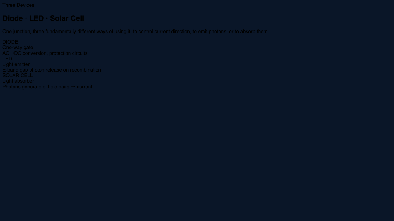
The LED: When electrons recombine with holes in certain semiconductor materials (like gallium arsenide), they release photons. The color of light depends on the material’s band gap — the energy difference between electron energy levels. Silicon’s band gap produces no visible light, which is why LEDs are made from compound semiconductors like GaAs (infrared), GaP (green), or InGaN (blue and white).
The solar cell: Light with energy greater than the band gap knocks electrons free in the depletion region, creating electron-hole pairs. The built-in electric field sweeps them to opposite sides of the junction, generating current without any battery. This is the photovoltaic effect — light to electricity, directly.
The Depletion Width: A Microscopic Geographer’s View
The width of the depletion region isn’t fixed — it depends on the doping concentrations and the applied voltage. For symmetric doping (N_A = N_D), the depletion width is:
W = √(2εVbi/eN)
Where ε is the semiconductor permittivity (ε_Si ≈ 11.7ε₀ for silicon), and N is the doping concentration. Heavily doped junctions have very narrow depletion regions; lightly doped junctions have wide ones. A wide depletion region is what lets solar cells absorb enough light to generate meaningful current — there’s more material where photon absorption can occur.
What the Interactive Graph Reveals
The PN junction visualization shows four panels simultaneously: the physical structure with the depletion region highlighted, the energy band diagram showing why the barrier forms, the current-voltage curve following the diode equation, and a carrier concentration plot showing how electron and hole densities vary across the junction.
The diode equation’s exponential behavior becomes immediately visible when you vary the voltage — the current barely changes from -0.2 V to 0.4 V, then climbs almost vertically from 0.5 V to 0.8 V. This sharp turn-on is why diodes are useful as voltage references: once the barrier is overcome, the voltage across the junction stabilizes near a predictable value.
The I-V curve also reveals the reverse-bias breakdown. At sufficiently negative voltages, the curve bends away from the flat, near-zero current line — avalanche breakdown kicks in. This is destructive at high currents, but deliberately exploited in Zener diodes, which are designed to break down at a specific, stable reverse voltage and used as voltage regulators.
Temperature, Band Gap, and Why Silicon Wins
The diode equation contains temperature explicitly. As T increases, the thermal voltage kT/e rises, which means the exponential grows more slowly — the turn-on voltage actually decreases with temperature, roughly -2 mV/°C for silicon. This is why the forward voltage of a diode is a rough thermometer: measure V at a known current, and you can estimate the junction temperature.
Silicon’s band gap (E_g ≈ 1.12 eV) is what makes it the dominant semiconductor. It’s large enough to give semiconductors their temperature stability and low leakage current, but small enough that thermal energy at room temperature (kT ≈ 0.026 eV) can be overcome with modest applied voltages. Germanium has a smaller band gap (~0.67 eV) and conducts at lower voltages but leaks too much current at high temperatures. Silicon strikes the right balance — which is why essentially all commercial semiconductors are silicon-based.
The Takeaway
The PN junction is one of those rare ideas that is both deeply fundamental and endlessly useful. Its behavior — the way a barrier forms, the way it lowers under forward bias and grows under reverse bias, the way it converts light to current and current to light — defines an entire technology civilization.
Next time you charge your phone, look at an LED clock, or read by the light of a panel, remember: somewhere in each device, electrons are crossing a boundary that humans learned to build, and the physics that makes it work was written into the structure of silicon itself.