
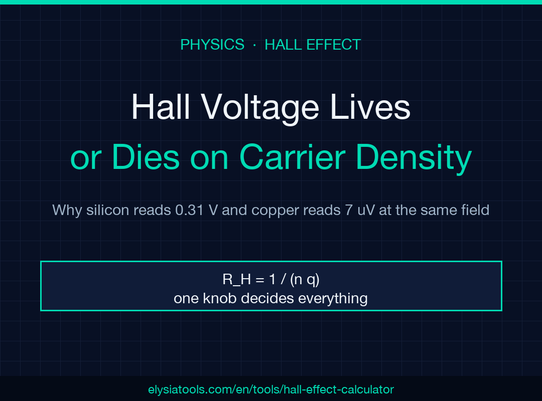
A 0.31 V signal at half a tesla versus seven microvolts at a full tesla: same equation, seven orders of magnitude apart. The Hall effect is the cleanest magnetic-field probe you can build with a four-terminal slab of doped silicon or a copper strip, and the only thing that decides whether your readback is a working sensor or a noise-floor whisper is one number, carrier density, sitting in the denominator of R_H = 1/(nq). Push n low enough (around 10²¹ m⁻³) and you get the workhorse configuration behind every phone magnetometer. Leave it at a metal’s natural density (around 10²⁸ m⁻³) and the Hall voltage vanishes into microvolts that no off-the-shelf ADC will resolve. This guide walks through the seven decisions that land your Hall voltage at the right magnitude for the job, drawn from real outputs of the Hall Effect Calculator.
The Hall voltage formula and why R_H = 1/(nq) is the only knob you need
The transverse voltage across a current-carrying conductor in a perpendicular magnetic field is:
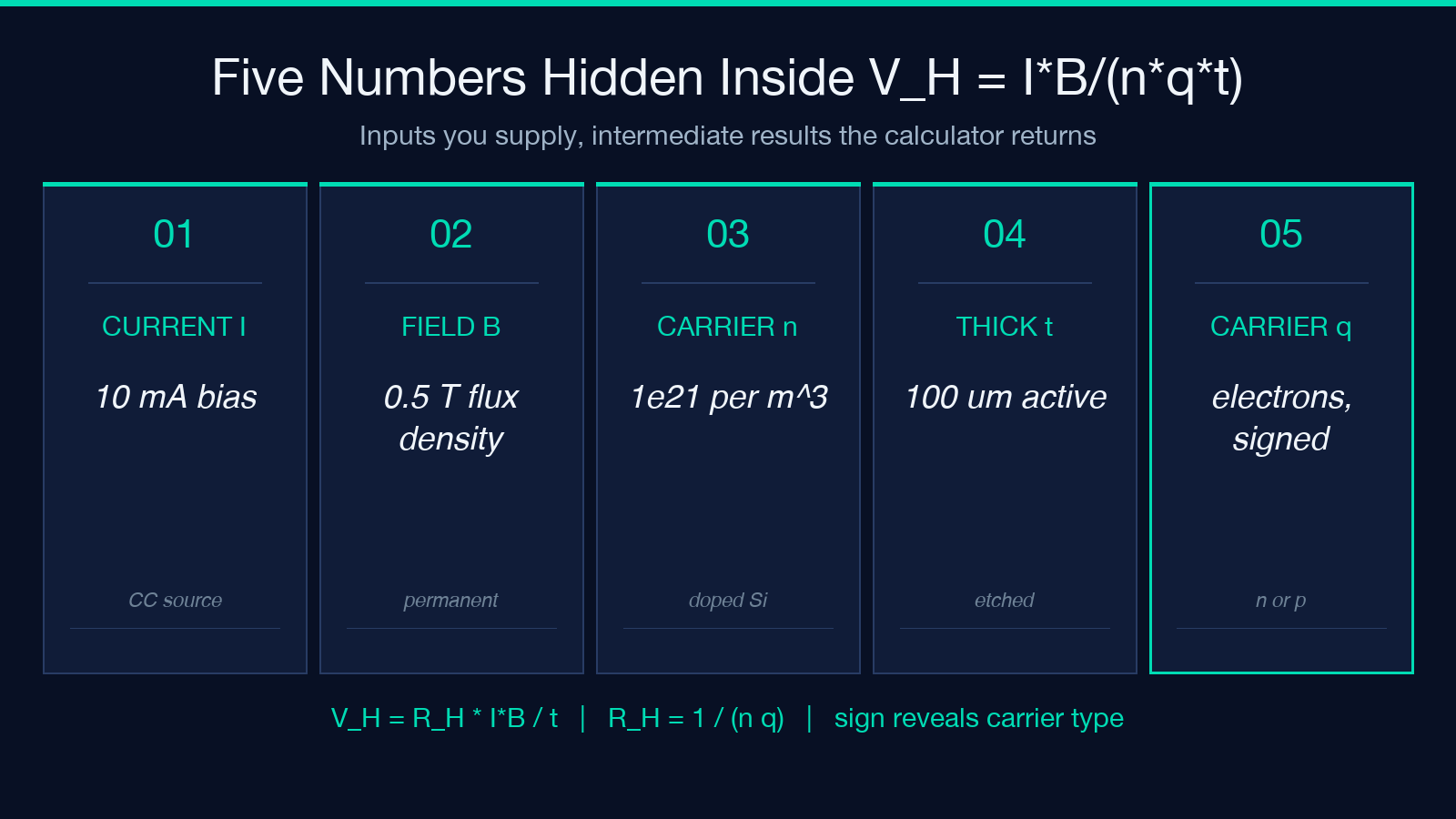
V_H = I B / (n q t) = R_H (I * B / t)with R_H = 1 / (n * q) the Hall coefficient, in cubic metres per coulomb. Three observations that drive every design choice downstream:
- – Carrier density
nis in the denominator — push it down by a factor of 100 andV_Hgoes up by 100. That single fact is why Hall sensors are built from semiconductors, not from metals. - – Carrier charge
qcarries a sign — electrons haveq = -e, holes haveq = +e. The sign ofV_Htells you whether your material is n-type or p-type, which is the cheapest carrier-identification test in solid-state physics. - – Thickness
tis the only geometric knob — halve the thickness and you double the voltage. That is why modern Hall elements are etched down to a few micrometres rather than milled from a chunk of ingot.
When you solve for R_H directly from a measured V_H, you can back out n and the carrier type. The reverse direction is what sensor designers actually run: pick R_H from the material, then size I, B, and t so V_H lands in a measurable band.
Three numbers on the inputs: current density, magnetic field, thickness
The numerical product that matters is I * B / t. Doubling any one of the three doubles V_H. Practical ranges you’ll see across real Hall elements:
- – Current
I: 1 mA to 20 mA for a silicon sense layer; 1 A to 10 A for a metal strip used only as a laboratory demonstration. - – Magnetic field
B: 0.01 T to 1 T for permanent-magnet proximity sensors; up to 10 T in cryogenic lab setups; the Earth’s field (50 µT) is essentially invisible to a copper-strip Hall probe. - – Thickness
t: 1 µm to 100 µm for an etched silicon layer; a few hundred micrometres for a metallic foil; the thinner the better, as long as the current path remains continuous.
The default anchor the calculator publishes — I = 10 mA, B = 0.5 T, t = 100 µm, n = 10²¹ m⁻³ — lands at V_H = -0.312 V with sensitivity -0.624 V/T. That is the configuration behind essentially every commercial Hall-effect switch and every phone magnetometer, because 0.3 V is trivially readable on any 3.3 V ADC.
The sign of V_H reveals the carrier type
Pick the carrier type from the dropdown before you run the calculation; the sign of V_H falls out automatically.
- – Electrons (n-type):
q = -e, soV_His negative. The deflection of electrons to one edge creates a positive charge on the opposite edge; conventional currentIand Hall electric fieldE_Hpoint in opposite directions. - – Holes (p-type):
q = +e, soV_His positive. Same deflection geometry, opposite sign of the charge carrier.
This is the cheapest carrier-identification test you can do in a teaching lab. Drive a fixed current, sweep a magnet over the sample, watch the polarity flip — and you’ve just told p-type silicon from n-type silicon without etching a single junction. The Van der Pauw geometry and Hall bars used in semiconductor research rely on this exact polarity rule.
Why metals fail and semiconductors work
Run the same calculation with copper, and the story collapses:
n_copper = 8.5e28 m^-3  (free electron density of Cu)
I = 10 A, B = 1 T, t = 100 um, carrier = electrons
V_H = -7.3 uV
Seven orders of magnitude on n, exactly seven orders of magnitude off on V_H. Even with 100× more current and 2× more field, the copper strip produces a signal three orders of magnitude smaller than the silicon layer. This is the single reason no commercial Hall element is built from a metal — and also the reason a Hall bar is the canonical demonstration of how dramatically material choice dominates geometry.
A useful sanity check: for any conductor with n > 10²⁶ m⁻³, expect V_H in the microvolt range under typical lab conditions. Anything you can plausibly solder to a board reads out as a millivolt or above — and that means semiconductor.
Sensitivity in V/T is the figure of merit for sensor design
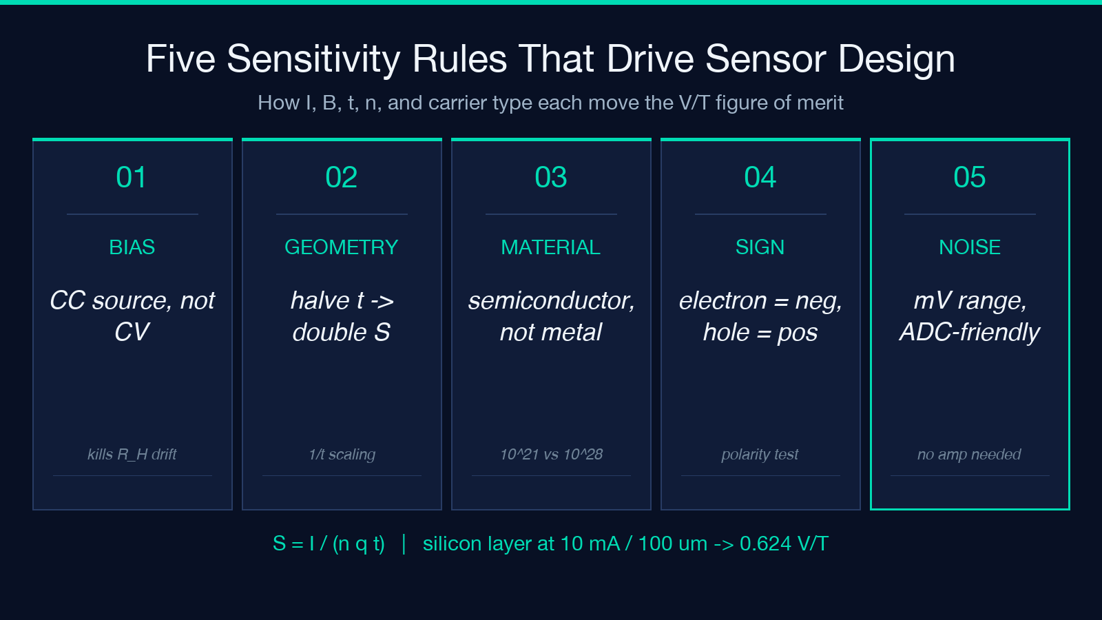
Sensitivity is S = V_H / B = I / (n q t), independent of the field you’re reading. For a fixed current and material, doubling t halves sensitivity. Doubling I doubles sensitivity. The silicon-layer anchor produces -0.624 V/T, which means a 1 mT field change reads as a 0.6 mV shift — easily resolved by any 12-bit ADC with a small front-end gain stage.
Two practical design rules:
- – Bias with a constant-current source, not a constant-voltage source. Temperature drift in
R_His significant for both silicon and III-V compounds; a CC source keepsI * Bclean whileR_Hdrifts. - – Use the thinnest active layer you can fabricate. Sensitivity scales as
1/t, so a 10 µm layer is 10× more sensitive than a 100 µm layer at the same current.
The carrier density unit trap: m^-3 vs cm^-3
Solid-state physics papers report n in cm⁻³; sensor datasheets and this calculator accept both. The conversion is a factor of 10⁶ (1 m⁻³ = 10⁻⁶ cm⁻³). Three places this trips people up:
– A silicon sense layer at n = 10²¹ m⁻³ is 10¹⁵ cm⁻³ — the canonical “lightly doped semiconductor” range. – A copper strip at n = 8.5 × 10²⁸ m⁻³ is 8.5 × 10²² cm⁻³ — a number you’ll see in solid-state textbooks. – An intrinsic silicon wafer at room temperature is around 10¹⁶ m⁻³ (= 10¹⁰ cm⁻³) — three orders of magnitude below the doped silicon above.
Forgetting the conversion gives an answer that is off by a factor of 10⁶, which looks like “the formula is broken” until you spot the unit. Run the calculator with both units if your input is suspicious; the output V_H will agree to four significant figures.
Temperature drift in R_H and the “calibrate at 25 °C” rule
Carrier density n is a function of temperature — for doped silicon the temperature coefficient is around 0.5 %/K near room temperature, and that drift multiplies directly into R_H. Three practical implications:
<ul> <li><strong>Calibrate at your operating temperature</strong>, not at room temperature, if your sensor runs above 50 °C or below 0 °C.</li> <li><strong>Use a differential measurement</strong> when the field is small: subtract a Hall-voltage reading at <code>B = 0</code> from the reading at <code>B = B₀</code> to cancel the offset drift.</li> <li><strong>Consider a spinning-current Hall IC</strong> for sub-mT precision; the IC flips the bias direction at a few kHz and synchronously detects, killing the offset term entirely.</li> </ul>
A Hall-effect switch used as a door sensor doesn’t care about drift because it only needs a binary threshold. A current sensor in a motor controller absolutely does — and that’s where the calibration discipline shows up.
Five practical rules when picking a Hall element
Five rules that capture the working knowledge above:
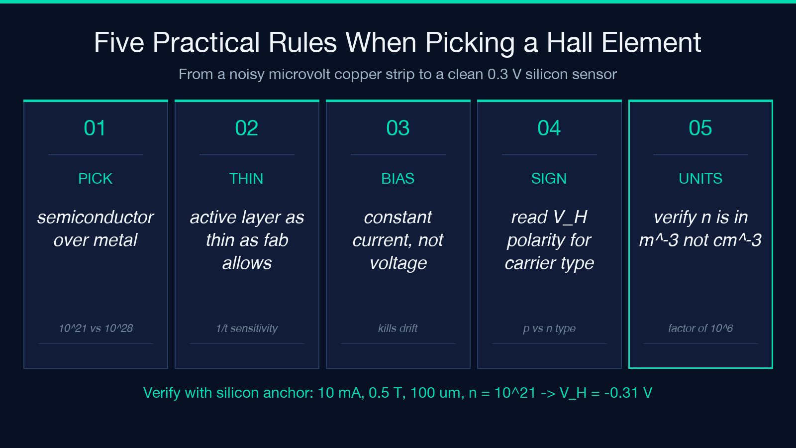
- – Pick semiconductor over metal for any sensor above microvolt precision. The 10²¹ vs 10²⁸ gap is unbridgeable.
- – Thin the active layer as much as your fab allows. Sensitivity scales as
1/t. - – Bias with a constant-current source so
R_Hdrift doesn’t leak into your readback. - – Read the sign of
V_Hto identify the carrier type — p-type flips positive, n-type stays negative. - – Verify
nin m⁻³ before trusting a literature value — the cm⁻³ / m⁻³ factor of 10⁶ is the most common silent error in Hall-effect analysis.
When in doubt, run a known anchor (silicon, 10 mA, 0.5 T, 100 µm, n = 10²¹ m⁻³) through the Hall Effect Calculator first; if you don’t land at V_H ≈ -0.31 V, the units are wrong, not the physics.
Wrap-up. The Hall effect reduces to a single ratio, R_H = 1/(nq), and the entire design problem is choosing materials and geometry so V_H = R_H I B / t lands in the readable band of your ADC. The seven orders of magnitude between silicon and copper on n is the whole reason sensors are made from semiconductors. Pick the carrier type, watch the sign, mind the units, and a four-terminal slab plus a magnet is enough to measure any field from the Earth’s 50 µT up to the 10 T cryogenic limit.
Explore more field-guide calculators across physics, electronics, and signal processing at elysiatools.com.
